- 您现在的位置:买卖IC网 > Sheet目录460 > IXTA160N10T (IXYS)MOSFET N-CH 100V 160A TO-263
�� �
�
�IXTA160N10T�
�IXTP160N10T�
�Symbol�
�Test� Conditions�
�Characteristic� Values�
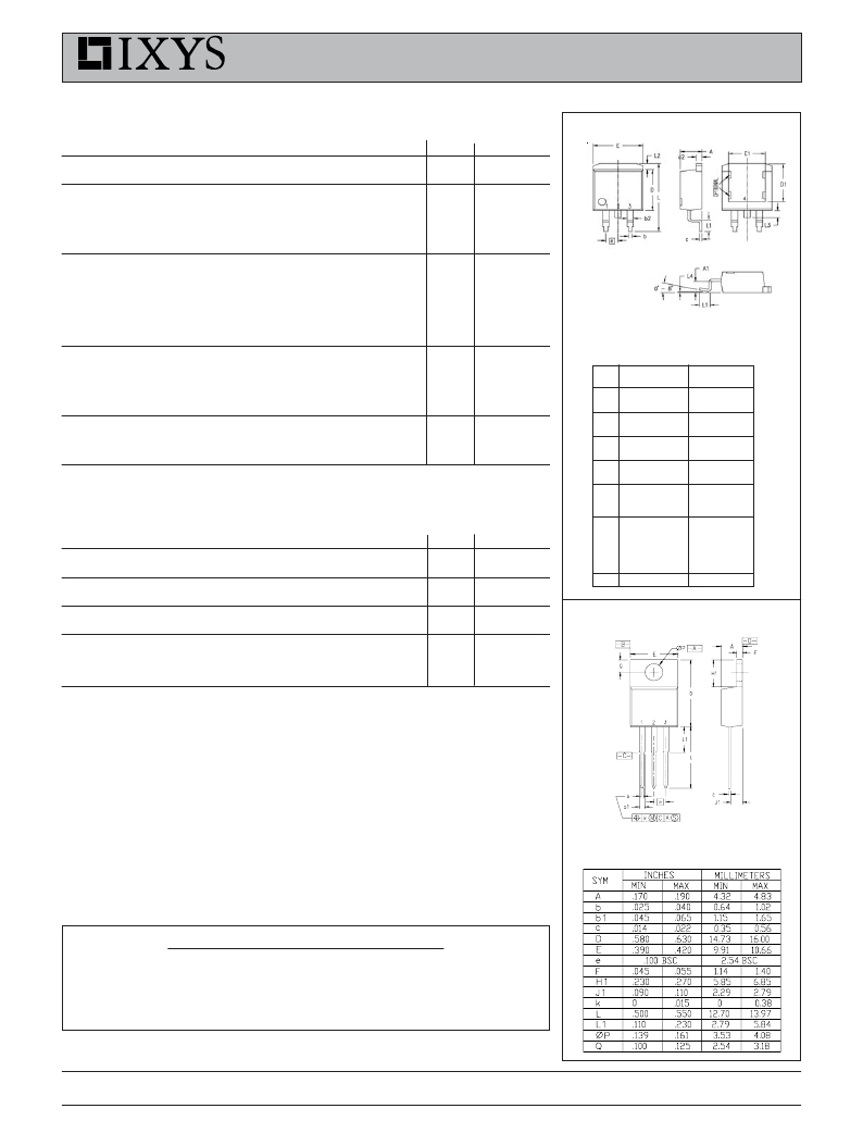
�TO-263� (IXTA)� Outline�
�(T� J� =� 25� °� C� unless� otherwise� specified)�
�Min.�
�Typ.�
�Max.�
�g� fs�
�C� iss�
�C� oss�
�C� rss�
�t� d(on)�
�t� r�
�V� DS� =� 10� V;� I� D� =� 60� A,� Note� 1�
�V� GS� =� 0� V,� V� DS� =� 25� V,� f� =� 1� MHz�
�Resistive� Switching� Times�
�V� GS� =� 10� V,� V� DS� =� 0.5� V� DSS� ,� I� D� =� 25� A�
�65�
�102�
�6600�
�880�
�135�
�33�
�61�
�S�
�pF�
�pF�
�pF�
�ns�
�ns�
�t� d(off)�
�t� f�
�R� G� =� 5� Ω� (External)�
�49�
�42�
�ns�
�ns�
�Pins:�
�1� -� Gate�
�3� -� Source�
�2� -� Drain�
�4,� TAB� -� Drain�
�Q� g(on)�
�Q� gs�
�Q� gd�
�V� GS� =� 10� V,� V� DS� =� 0.5� V� DSS� ,� I� D� =� 25� A�
�132�
�37�
�40�
�nC�
�nC�
�nC�
�Dim.�
�A�
�A1�
�Millimeter�
�Min.� Max.�
�4.06� 4.83�
�2.03� 2.79�
�Inches�
�Min.� Max.�
�.160� .190�
�.080� .110�
�R� thJC�
�R� thCH�
�TO-220�
�0.50�
�0.35� °� C/W�
�°� C/W�
�b�
�b2�
�c�
�c2�
�0.51�
�1.14�
�0.46�
�1.14�
�0.99�
�1.40�
�0.74�
�1.40�
�.020�
�.045�
�.018�
�.045�
�.039�
�.055�
�.029�
�.055�
�D�
�D1�
�8.64�
�7.11�
�9.65�
�8.13�
�.340�
�.280�
�.380�
�.320�
�Source-Drain� Diode�
�E�
�E1�
�e�
�9.65�
�6.86�
�2.54�
�10.29�
�8.13�
�BSC�
�.380�
�.270�
�.100�
�.405�
�.320�
�BSC�
�Symbol� Test� Conditions�
�T� J� =� 25� °� C� unless� otherwise� specified)�
�Characteristic� Values�
�Min.� Typ.� Max.�
�L�
�L1�
�L2�
�14.61�
�2.29�
�1.02�
�15.88�
�2.79�
�1.40�
�.575�
�.090�
�.040�
�.625�
�.110�
�.055�
�I� S�
�V� GS� =� 0� V�
�160�
�A�
�L3�
�L4�
�1.27�
�0�
�1.78�
�0.38�
�.050�
�0�
�.070�
�.015�
�I� SM�
�Pulse� width� limited� by� T� JM�
�430�
�A�
�R�
�0.46�
�0.74�
�.018�
�.029�
�V� SD�
�t� rr�
�I� F� =� 25� A,� V� GS� =� 0� V,� Note� 1�
�I� F� =� 25� A,� -di/dt� =� 100� A/� μ� s�
�60�
�1.0�
�V�
�ns�
�TO-220� (IXTP)� Outline�
�V� R� =� 50� V,� V� GS� =� 0� V�
�Notes:� 1.� Pulse� test,� t� ≤� 300� μ� s,� duty� cycle� d� ≤� 2� %;�
�2.� On� through-hole� packages,� R� DS(on)� Kelvin� test� contact�
�location� must� be� 5� mm� or� less� from� the� package� body.�
�PRELIMINARYTECHNICALINFORMATION�
�The� product� presented� herein� is� under� development.� The� Technical� Specifications� offered�
�are� derived� from� data� gathered� during� objective� characterizations� of� preliminary� engineering�
�lots;� but� also� may� yet� contain� some� information� supplied� during� a� pre-production� design�
�evaluation.� IXYS� reserves� the� right� to� change� limits,� test� conditions,� and� dimensions�
�without� notice.�
�IXYS� reserves� the� right� to� change� limits,� test� conditions,� and� dimensions.�
�Pins:�
�1� -� Gate�
�3� -� Source�
�2� -� Drain�
�4,� TAB� -� Drain�
�IXYS� MOSFETs� and� IGBTs� are� covered� by�
�one� or� moreof� the� following� U.S.� patents:�
�4,835,592�
�4,850,072�
�4,881,106�
�4,931,844�
�5,017,508�
�5,034,796�
�5,049,961�
�5,063,307�
�5,187,117�
�5,237,481�
�5,381,025�
�5,486,715�
�6,162,665�
�6,259,123� B1�
�6,306,728� B1�
�6,404,065� B1�
�6,534,343�
�6,583,505�
�6,683,344�
�6,710,405� B2�
�6,710,463�
�6,727,585�
�6,759,692�
�6,771,478� B2�
�7,005,734� B2�
�7,063,975� B2�
�7,071,537�
�发布紧急采购,3分钟左右您将得到回复。
相关PDF资料
IXTA180N085T7
MOSFET N-CH 85V 180A TO-263-7
IXTA180N085T
MOSFET N-CH 85V 180A TO-263
IXTA180N10T7
MOSFET N-CH 100V 180A TO-263-7
IXTA180N10T
MOSFET N-CH 100V 180A TO-263
IXTA182N055T7
MOSFET N-CH 55V 182A TO-263-7
IXTA182N055T
MOSFET N-CH 55V 182A TO-263
IXTA1R4N100P
MOSFET N-CH 1000V 1.4A TO-263
IXTA1R4N120P
MOSFET N-CH 1200V 1.4A TO-263
相关代理商/技术参数
IXTA160N10T7
功能描述:MOSFET 160 Amps 100V 6.9 Rds RoHS:否 制造商:STMicroelectronics 晶体管极性:N-Channel 汲极/源极击穿电压:650 V 闸/源击穿电压:25 V 漏极连续电流:130 A 电阻汲极/源极 RDS(导通):0.014 Ohms 配置:Single 最大工作温度: 安装风格:Through Hole 封装 / 箱体:Max247 封装:Tube
IXTA16N50P
功能描述:MOSFET 16.0 Amps 500 V 0.4 Ohm Rds RoHS:否 制造商:STMicroelectronics 晶体管极性:N-Channel 汲极/源极击穿电压:650 V 闸/源击穿电压:25 V 漏极连续电流:130 A 电阻汲极/源极 RDS(导通):0.014 Ohms 配置:Single 最大工作温度: 安装风格:Through Hole 封装 / 箱体:Max247 封装:Tube
IXTA170N075T2
功能描述:MOSFET 170 Amps 75V RoHS:否 制造商:STMicroelectronics 晶体管极性:N-Channel 汲极/源极击穿电压:650 V 闸/源击穿电压:25 V 漏极连续电流:130 A 电阻汲极/源极 RDS(导通):0.014 Ohms 配置:Single 最大工作温度: 安装风格:Through Hole 封装 / 箱体:Max247 封装:Tube
IXTA180N055T
功能描述:MOSFET 180 Amps 55V 0.004 Ohm Rds RoHS:否 制造商:STMicroelectronics 晶体管极性:N-Channel 汲极/源极击穿电压:650 V 闸/源击穿电压:25 V 漏极连续电流:130 A 电阻汲极/源极 RDS(导通):0.014 Ohms 配置:Single 最大工作温度: 安装风格:Through Hole 封装 / 箱体:Max247 封装:Tube
IXTA180N085T
功能描述:MOSFET 180 Amps 85V 5.5 Rds RoHS:否 制造商:STMicroelectronics 晶体管极性:N-Channel 汲极/源极击穿电压:650 V 闸/源击穿电压:25 V 漏极连续电流:130 A 电阻汲极/源极 RDS(导通):0.014 Ohms 配置:Single 最大工作温度: 安装风格:Through Hole 封装 / 箱体:Max247 封装:Tube
IXTA180N085T7
功能描述:MOSFET 180 Amps 85V 5.5 Rds RoHS:否 制造商:STMicroelectronics 晶体管极性:N-Channel 汲极/源极击穿电压:650 V 闸/源击穿电压:25 V 漏极连续电流:130 A 电阻汲极/源极 RDS(导通):0.014 Ohms 配置:Single 最大工作温度: 安装风格:Through Hole 封装 / 箱体:Max247 封装:Tube
IXTA180N10T
功能描述:MOSFET 180 Amps 100V 6.1 Rds RoHS:否 制造商:STMicroelectronics 晶体管极性:N-Channel 汲极/源极击穿电压:650 V 闸/源击穿电压:25 V 漏极连续电流:130 A 电阻汲极/源极 RDS(导通):0.014 Ohms 配置:Single 最大工作温度: 安装风格:Through Hole 封装 / 箱体:Max247 封装:Tube
IXTA180N10T7
功能描述:MOSFET 180 Amps 100V 6.1 Rds RoHS:否 制造商:STMicroelectronics 晶体管极性:N-Channel 汲极/源极击穿电压:650 V 闸/源击穿电压:25 V 漏极连续电流:130 A 电阻汲极/源极 RDS(导通):0.014 Ohms 配置:Single 最大工作温度: 安装风格:Through Hole 封装 / 箱体:Max247 封装:Tube